
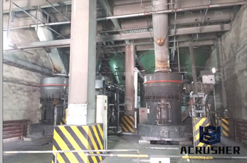
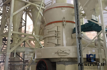
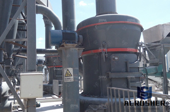
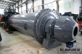
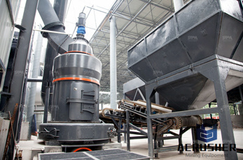
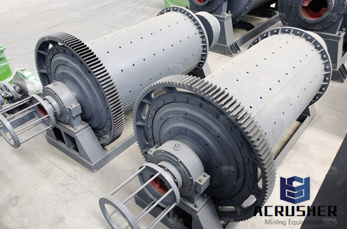
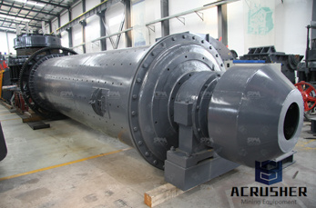
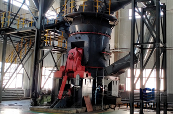
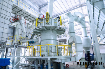
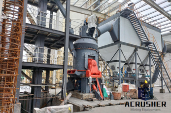
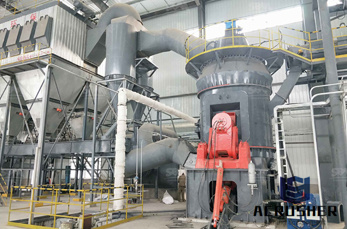
silicon wafer backgrinding process manufacturer Grasping strong production capability, advanced research strength and excellent service, Shanghai silicon wafer backgrinding process supplier create the value and bring values to all of customers.
 WhatsApp)
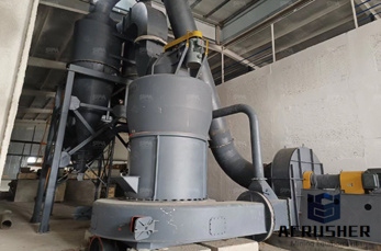
Wafer backgrinding is a semiconductor device fabrication step during which wafer thickness is reduced to allow stacking and highdensity packaging of integrated circuits (IC).. ICs are produced on semiconductor wafers that undergo a multitude of processing steps. The silicon wafers predominantly used today have diameters of 200 and 300 mm. They are roughly 750 μm thick to ensure a minimum .
Back End(BE) Process Wafer Sawing(Dicing Saw) • Process by which individual silicon chips (die) are separated from each other on the wafer. • Get the wafer cut per each lines with the (Deionized) water to prevent any electrostatic issue or contamination. Silicon wafer Sawing blade Sawing blade Silicon wafer Before After
Prior to IC packaging, the wafer is ground to final thickness in a "backgrinding" process. Large amounts of ultrapure water are used for rinsing off the fine silicon particles and cooling the wafer during the grinding operation and this is discharged from the wafer packaging facility.
Meister Abrasives'' micro grit product range used for fine grinding of prime wafers or back thinning applications are capable of achieving surface finishes in the angstrom range. Ceramet hybrid and vitrified bonded grinding wheels create a quantum leap in photovoltaic grinding process efficiency. Prime wafer manufacturing
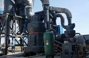
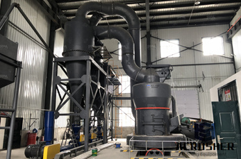
Wafer Backgrind Wafer Backgrind is the process of grinding the backside of the wafer to the correct wafer thickness prior to assembly. It is also referred to as ''wafer thinning.'' Wafer backgrinding has not always been necessary, but the drive to make packages thinner and thinner has made it indispensable.

Fine grinding of silicon wafers requires using #2000 mesh (3–6 µm grit size) or fi ner diamond wheels. The surfaces to be fi ne ground generally have no damage or very little damage and the surface roughness is 30 nm in Ra [6]. The uniqueness and the special requirements of silicon wafer fi ne grinding process were discussed in the pre
After the wafers have been sliced, the lapping process begins. Lapping the wafer removes saw marks and surface defects from the front and backside of the wafer. It also thins the wafer and helps to relieve stress accumulated in the wafer from the slicing process. After lapping the silicon wafers, they go through an etching and cleaning process.
Jan 15, 2013· Silicon dies are separated from the wafer via a dicing or sawing process. Typically, wafers coming out of the foundry are approximately 750um thick to ensure maximum robustness during shipping. Before dicing wafers typically go through a back grinding (or backgrinding) process to thin down wafers to 75um to 50um.
Wafer backgrinding starts with a large grit wheel to remove most of the surface, and wheels with a finer grit are used to finish polishing the silicon wafer to the desired thickness. To prevent contamination, deionized water is used to wash debris from the surface throughout the wafer thinning process.
Ultrathin silicon wafer technology is reviewed in terms of the semiconductor applications, critical challenges, and wafer preassembly and assembly process technologies and their underlying ...
prethinned silicon carrier wafers with a diameter of 200 ± mm were thinned on a DISCO DFG8540 grinder. The large silicon carrier wafers were from MEMC and had a diameter of ± mm. The device wafers that were bonded to the large carrier wafers had a diameter of 200 ± mm. The edgetrimming process was done on a
Grinding of silicon wafers: A review from historical perspectives. ... The process is also used for " backgrinding " after microfabrication where the substrate thickness is reduced to a ...
This study investigates warping of silicon wafers in ultraprecision grindingbased backthinning process. By analyzing the interactions between the wafer and the vacuum chuck, together with the machining stress distributions in damage layer of ground wafer, the study establishes a mathematical model to describe wafer warping during the thinning process using the elasticity theory.
QuikPak, originally founded in 1994 as SPT, was purchased by Delphon Industries in 2000. For the last 15 years, QuikPak has provided fast turn IC Packaging, Assembly, Prototype and Wafer Processing Services to a wide variety of Semiconductor and Electronics Companies, as well as major Military and Aerospace institutions.
The backgrinding operation, sometimes called thinning, is where the silicon wafers, 20 to 30cm in diameter, are reduced in thickness from approximately 750µ to around 20 to 30µ, sometimes considerably less. Grinding wheels, impregnated of various .
Etching is used in microfabrication to chemically remove layers from the surface of a wafer during manufacturing. Etching is a critically important process module, and every wafer undergoes many etching steps before it is complete. For many etch steps, part of the wafer is protected from the etchant by a "masking" material which resists etching.
Back grinding is a process that removes silicon from the back surface of a wafer. Silicon Valley Microelectronics provides grinding on our own substrates or on customer supplied wafers. We process bare and device patterned wafers with high yield and offer wafer thinning to customer specifications. SVM Wafer Back Grinding Capabilities:
Syagrus Systems is a leader in postfab for semiconductor and electronic components by providing silicon wafer backgrinding, wafer dicing, die inspection and sorting, and SMD Tape and Reel.
Silicon Wafer Backgrinding Process. Wafer backgrind wafer backgrind is the process of grinding the backside of the wafer to the correct wafer thickness prior to assemblyt is also referred to as wafer thinning wafer backgrinding has not always been necessary, but the drive to make packages thinner and thinner has made it indispensable.
We routinely process LED and MEMS devices. QuikPak utilizes stateoftheart equipment from Disco, Ultron and Royce to offer the following services, which are performed inhouse in as little as one day: Additional services provided by QuikPak include: Wafer Backgrinding or Thinning; Dicing of Silicon, Glass, Quartz, Laminate, Ceramic and Panels
Silicon Wafer Processing Thinning and Dicing In the manufacturing of semiconductor wafers and integrated circuits, backgrinding is one of the most important processes. Incoming wafers from wafer fabrication plants usually are in the range of 700 to 800um. It is necessary to thin these wafers to the required thickness to cater for low package ...
NOVEL ULTRAFILTRATION OPERATING PROCESS FOR SILICON WAFER PRODUCTION WASTEWATER REUSE Ben Freeman Hydranautics – A Nitto Group Company ... Backgrinding + Dicing WW (left) and Dicing WW only (right) AWWA/AMTA© 6. Ultrapure Water Process . .
Sep 03, 2017· Wafer backgrinding is a semiconductor device fabrication step during which wafer thickness is reduced to allow for stacking and high density packaging of integrated circuits (IC).
Backgrinding is the process of removal of silicon from the back of wafers following conventional semiconductor processing. The process is primarily utilized in thinning wafers for commercial semiconductor wafer fabs. Wafers are first laminated using an automatic taping machine. After inspection, they are placed on a Disco 84X series infeed grinder.
WhatsApp)